Prof. Aram Amassian Speaks at The Upcoming ORaCEL Seminar on the topic of Semiconductor Inks
Semiconductor Inks: The Next Maker Revolution?
Prof. Aram Amassian
Department of Materials Science and Engineering, and ORaCEL, NCSU.
E-mail: aamassi@ncsu.edu
Group Website
Date: Monday August 27, 2018
Venue: Toxicology Auditorium 2104
Time: 11:00 AM.
Abstract
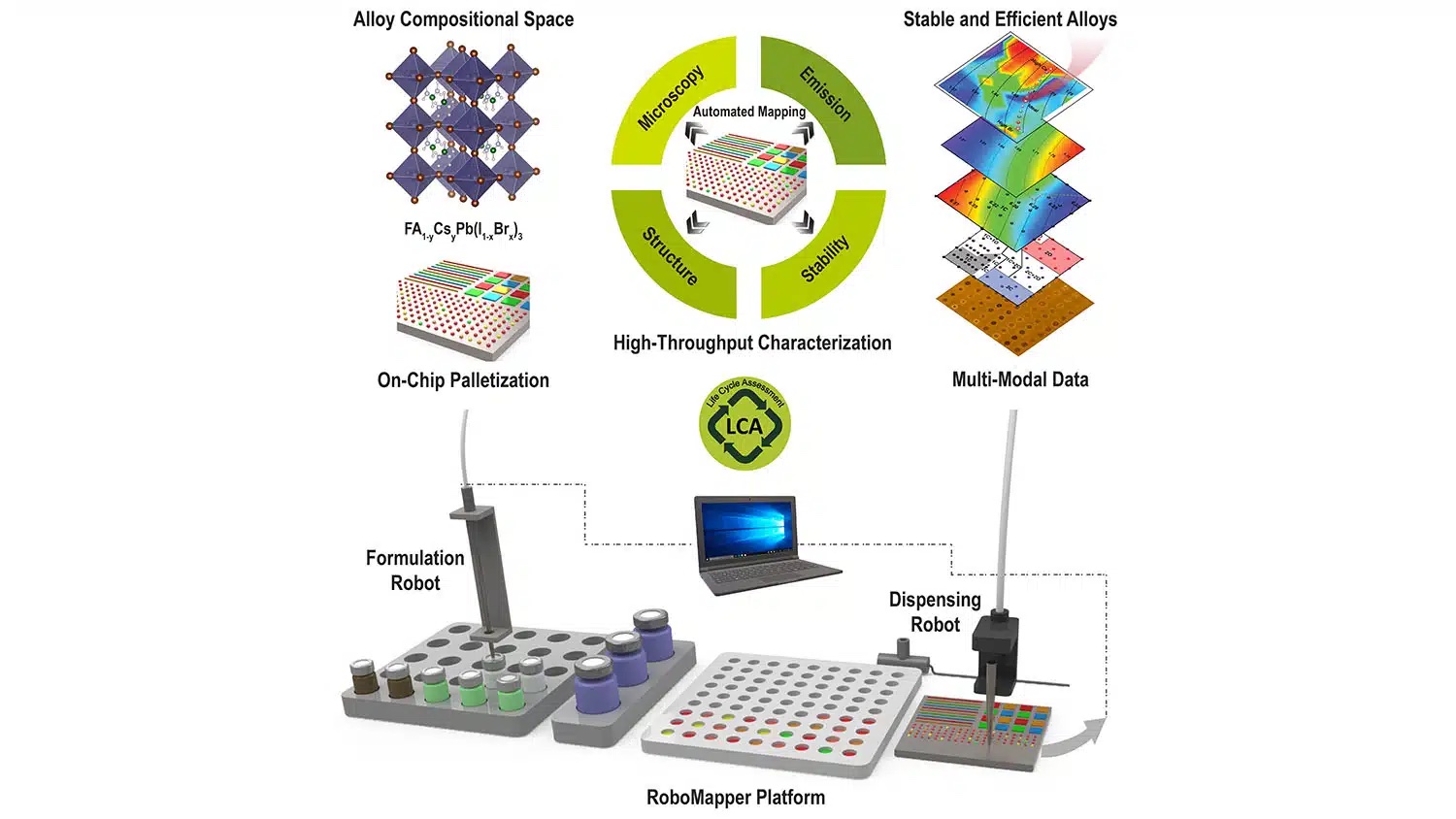
Additive manufacturing of commodity materials has made significant inroads in recent years. In addition to transforming the way many industries do prototyping, it is developing into a viable manufacturing technique. Meanwhile, low-cost additive manufacturing in ambient air, such as 3D printing of bulk plastics, has already started a Maker movement and is transforming the way we design, create, innovate and educate. In the future, the ability to print and coat semiconductors and other building blocks of modern technology can create similar opportunities for industry and for a new generation of technically savvy Makers. Modern semiconductors, some of which are carbon-based, also combine several highly desirable features making them amenable to additive manufacturing. Ink-based semiconductors that come to mind today include conjugated molecules and polymers, colloidal quantum dots, metal halide (a.k.a. perovskites) and transition metal oxides. These materials form an ink (solution/suspension/sol-gel) that can be applied and dried in ambient air to form in some instances remarkably high quality materials that have the potential to not only displace incumbent materials and fabrication processes, but to create new opportunity spaces and design form factors in the future.
In this presentation, I will introduce the current understanding of ink-based manufacturing of organic and hybrid perovskite semiconductor films through examples. These examples will be presented through time-resolved studies of the solidification to link the solid-state microstructure and device figures of merit to the ink’s formulation, drying conditions and the solidification process. Recent developments in ink formulation and processing that enable ambient fabrication of high quality semiconductor films and macroscopic single crystals will also be presented, along with examples of their integration in state-of-the-art electronic and photovoltaic devices.
Biography:  Aram Amassian is an Associate Professor of Materials Science and Engineering and a founding member of the Carbon Electronics Cluster at the North Carolina State University. Aram obtained his PhD in Engineering Physics from Ecole Polytechnique (Montreal, Canada) in 2006, and was subsequently a postdoctoral fellow in Materials Science and Engineering at Cornell University, working with George Malliaras. He was appointed Assistant Professor of Materials Science and Engineering in 2009 at the King Abdullah University of Science and Technology (KAUST), and was one among nearly 75 founding faculty. He has been awarded the NSERC Postdoctoral Fellowship, as well as the American Vacuum Society’s Electronic Materials Postdoctoral Award and was the Career Development SABIC Chair from 2013-2015 for his work on solution processed optoelectronic materials. His research focus is aimed at enabling the ink-based additive manufacturing of electronic, optoelectronic and photovoltaic devices based on a variety of emerging semiconductor materials, including organic, quantum dot and hybrid organic-inorganic perovskites. He is best known for in-depth in situ characterization of materials growth. His work has been supported by industry, including by Boeing and SABIC, and spans collaborations in the US, Canada, Asia, Europe and the UK. He has co-authored more than 160 publications in peer reviewed journals and has delivered over 100 invited talks and seminars.